- 您现在的位置:买卖IC网 > Sheet目录335 > ISO1I811T (Infineon Technologies)ISOLAT DGTL 500VAC 8CH 48TSSOP
ISO1I811T
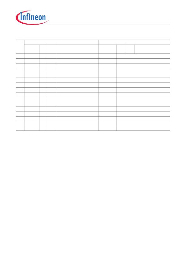
Pin Configuration and Functionality
1
Pin Configuration and Functionality
The pin configuration slightly differs for the parallel or the serial interface.
1.1
Pin Configuration
The ordering, type and functions of the IC pins are listed in the Table 1 .
Table 1
Pin Configuration
Pin
Parallel Interface Mode
Serial Interface Mode
Symbol
Ctrl Type Function
1)
2)
Symbol
Ctrl. Type Function
1
GND
A
Logic Ground
GND
2
3
SEL
n.c.
I
PU
Serial Parallel Mode Select
not connected
SEL
n.c.
4
ROSC
A
Clock Frequency Adjustment ROSC
5
VCC
A
Positive 5/3.3V logic supply
VCC
6
ERR
O
OD,
Error output
ERR
PU
7
GND
A
Logic Ground
GND
8
D0
O
PPZ
Data output bit0
SDI
I
PD
SPI Data input
9
10
11
12
D1
D2
D3
D4
O
O
O
O
PPZ
PPZ
PPZ
PPZ
Data output bit1
Data output bit2
Data output bit3
Data output bit4
GND
GND
GND
GND
13
D5
O
PPZ
Data output bit5
SCLK
I
PD
SPI Shift Clock input
14
D6
O
PPZ
Data output bit6
GND
15
D7
O
PPZ
Data output bit7
SDO
O
PPZ
SPI Data output
16
CS
I
PU
Chip Select
CS
17
18
19
20
21
RD
GND
DS0
DS1
GND
I
I
I
PU
A
PD
PD
A
Data Read Input
Logic Ground
Filter Select Input 0
Filter Select Input 1
Logic Ground
n.c.
GND
DS0
DS1
GND
not connected
22
23
n.c.
n.c.
not connected
not connected
n.c.
n.c.
24
25
GND
GNDBB
A
A
Logic Ground
Input Ground
GND
GNDBB
26
VBB
A
Positive input supply voltage VBB
27
28
29
30
31
32
I0L
I0H
I1L
I1H
GNDBB
I2L
A
A
A
A
A
A
Input 0 Low, LED Out
Input 0 High
Input 1 Low, LED Out
Input 1 High
Input Ground
Input 2 Low, LED Out
I0L
I0H
I1L
I1H
GNDBB
I2L
Data Sheet
6
Revision 2.0, 2012-06-14
发布紧急采购,3分钟左右您将得到回复。
相关PDF资料
ISO7221AQDRQ1
IC DGTL ISOLATOR 1MBPS DL 8SOIC
ISOBAR4 ULTRA
SURGE SUPPRSSR 4OUT 6'CORD W/LED
ISOBAR6 ULTRA
SURGE SUPPRSSR 6OUT 6'CORD W/LED
ISOBAR6DBS
SURGE SUPP DSS 6OUT 6'CORD W/LED
ISOBAR6ULTRAHG
SURGE SUPP 6OUT 15'CORD HOSP GRD
ISOBAR6
SURGE SUPPRSSR 6OUT 6'CORD
ISOBAR8 ULTRA
SURGE SUPPR 8OUT 12'CORD W/LED
ISOBLOK2-0
SURGE SUPP ISOBAR 2 OUT/DIRECT
相关代理商/技术参数
ISO1I811TXUMA1
制造商:Infineon Technologies AG 功能描述:ISOFACE - Tape and Reel 制造商:Infineon Technologies AG 功能描述:IC DGTL ISO 8CH PAR SER 48TSSOP
ISO1I811TXUMA1/SAMPLE
制造商:Infineon Technologies AG 功能描述:ISOFACE - Tape and Reel
ISO1I813T
功能描述:ISOLATOR DGTL 500VAC 8CH 48TSSOP RoHS:是 类别:隔离器 >> 数字隔离器 系列:ISOFACE™ 标准包装:66 系列:iCoupler® 输入 - 1 侧/2 侧:2/2 通道数:4 电源电压:3.3V,5V 电压 - 隔离:2500Vrms 数据速率:25Mbps 传输延迟:60ns 输出类型:逻辑 封装/外壳:20-SSOP(0.209",5.30mm 宽) 供应商设备封装:20-SSOP 包装:管件 工作温度:-40°C ~ 105°C
ISO1I813TXUMA1
制造商:Infineon Technologies AG 功能描述:Isolated 8 Channel Digital Input 48-Pin TSSOP 制造商:Infineon Technologies AG 功能描述:ISOFACE - Tape and Reel 制造商:Infineon Technologies AG 功能描述:ISOLATOR DGTL 500VAC 8CH 48TSSOP
ISO2
制造商:未知厂家 制造商全称:未知厂家 功能描述:ASIC
ISO212
制造商:BB 制造商全称:BB 功能描述:Low Cost, Two-Port Isolated, 1500Vrms ISOLATION AMPLIFIER
ISO212JP
制造商: 功能描述: 制造商:undefined 功能描述:
ISO212JP-15
制造商:BB 制造商全称:BB 功能描述:Low Cost, Two-Port Isolated, 1500Vrms ISOLATION AMPLIFIER
